DDR4 Verification IP 项目
功能概述
本项目的主要目的是使用 System Verilog 设计和测试 DDR4 控制器以及高速接口。该项目分为三个主要模块:
一、DDR4 控制器接口:提供将命令、数据转换为 DDR 控制器和内存 DDR4 DIMM 使用的引脚信号电平;
二、DDR 控制器:它被构建为一个 RTL 行为模型,并迭代转换为可综合模块。
三、DIMM 模组和其他部件,它们在测试台中用于验证 DDR 接口。
设计框图
信号逻辑图
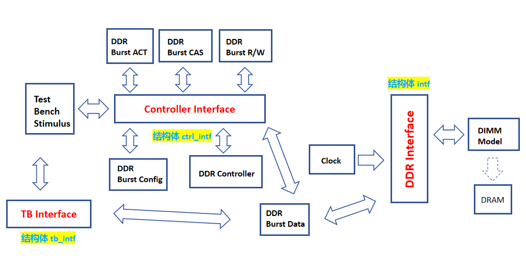
对于时钟 其实各个.sv 都具有联系
文件清单
| Folder | File | Description |
|---|---|---|
| burst_conf.sv | DDR4 Initialization Sequence Configuration Module | |
| burst_act.sv | Act Row Address Checking and Handling Module | |
| burst_cas.sv | Modules to handle CAS-related delays, e.g. tRCD, tCCD | |
| burst_rw.sv | Read/Write Latency Control Module | |
| burst_data.sv | Pin Signal Acquisition and Conversion Module with Data, Addresses for Read/Write and MRS Processes | |
| ctrl_interface.sv | Interfaces for submodules and control signals related to the DDR controller | |
| ddr_controller.sv | DDR4 controller main FSM module for initialization, read/write, and refresh operations | |
| ddr_clock.sv | Differential Clock and DQS Generation Module | |
| ddr_interface.sv | DDR4 interface module for connecting the DDR4 controller to the behavioral model | |
| dimm_model.sv | DDR4 DIMM model for implementing pin sampling, capture ACT and CAS commands | |
| ddr_package.pkg | DDR4 controller data types and parameter definitions | |
| ddr_top.sv | DDR4 Controller Top-Level Module | |
| memory_check.sv | Capture read/write requests in random incentives and save the data information of each read/write address and compare it at the final output moment for statistical verification of Pass and Fail conditions | |
| Rand_Stimulus.sv | Random read/write, data stimulus generation module, used to generate random read/write addresses and data | |
| tb_interface.sv | Connection interface between DDR4 controller, DIMM model, and memory checking module | |
| ddr_genvector.sv | DDR4 Simulation Vector Generation Module | |
| tb | test.sv | Testbench top module |
| sim | ddr4_tb.f | Simulation file list |
| Makefile | VCS/Verdi Automation Simulation Scripts |
DDR 控制器模块 (ddr_controller.sv)
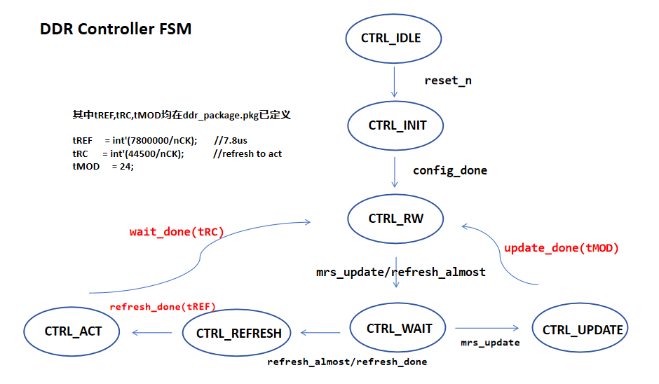
模块实现了图所示的 FSM ,可以完成初始化、读/写、刷新和更新等基础控制。
复位时,状态机开始进入 INIT 状态。INIT 状态将启动模式寄存器设置序列,以设置 DDR 操作。 然后保持 RW 状态,进行突发读/写操作。
模块实现了一个定时器来跟踪 tREF。 当定时器接近到期时,FSM 将向内存管理单元(MMU)或本例中的刺激发生器发出 dev_busy 信号,以停止发送请求并完成所有读写操作。控制器向 DIMM 发出刷新命令,并在 tRC 延迟后返回 RW 状态。
控制器还为 MMU 提供了将 8 字节突发长度和 4 字节突发长度的双向切换。 控制器发出信号停止接收任何请求,并完成当前所有操作,然后开始通过命令 MR0 将 DIMM 设置为新的突发长度。
DDR初始化 (burst_conf.sv)
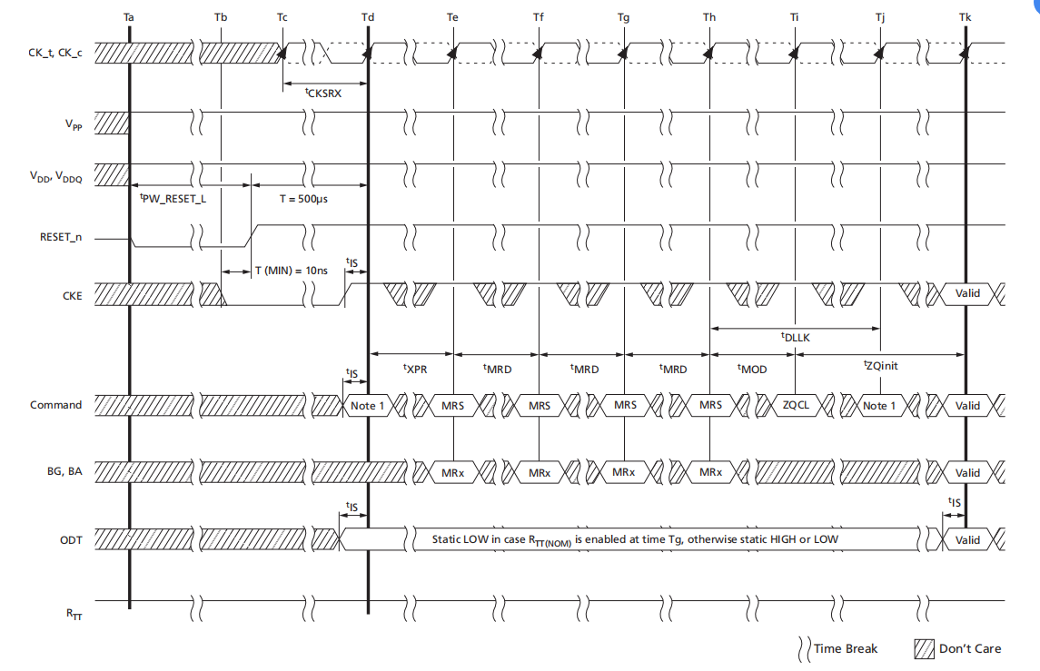
该模块实现了向 DIMM 发送初始化命令的序列,以便在复位和 CKE 引脚后设置操作。该序列通过 SV 任务实现,设置时序在该模块和顶层模块中设置了参数。 设置时序可以在不修改代码的情况下,根据其实例进行更改。
参考<<8Gb: x8, x16 Automotive DDR4 SDRAM>>PDF RESET and Initialization Procedure章节,配置时序与模式寄存器内容。
…… 设置电压相关的
After RESET_n is de-asserted, wait for another 500μs but no longer then 3 seconds until CKE becomes active. During this time, the device will start internal state initialization; this will be done independently of external clocks. A reasonable at tempt was made in the design to power up with the following default MR settings: gear-down mode (MR3 A[3]): 0 = 1/2 rate; per-DRAM addressability (MR3 A[4]): 0= disable; maximum power-down (MR4 A[1]): 0 = disable; CS to command/address latency (MR4 A[8:6]): 000 = disable; CA parity latency mode (MR5 A[2:0]):000 = disable. However, it should be assumed that at power up the MR settings are undefined and should be programmed as shown below.
Clocks (CK_t, CK_c) need to be started and stabilized for at least 10ns or 5 tCK (whichever is larger) before CKE goes active. Because CKE is a synchronous signal, the corresponding setup time to clock (tIS) must be met. Also, a DESELECT com mand must be registered (with tIS setup time to clock) at clock edge Td. After the CKE is registered HIGH after RESET, CKE needs to be continuously registered HIGH until the initialization sequence is finished, including expiration of t DLLK and t ZQinit.
The device keeps its ODT in High-Z state as long as RESET_n is asserted. Further,the SDRAM keeps its ODT in High-Z state after RESET_n de-assertion until CKE isregistered HIGH. The ODT input signal may be in an undefined state until t IS before CKE is registered HIGH. When CKE is registered HIGH, the ODT input signalmay be statically held either LOW or HIGH. If RTT(NOM) is to be enabled in MR1,the ODT input signal must be statically held LOW. In all cases, the ODT input signal remains static until the power-up initialization sequence is finished, including the expiration of t DLLK and t ZQinit.
After CKE is registered HIGH, wait a minimum of RESET CKE EXIT time, t XPR, before issuing the first MRS command to load mode register (tXPR = MAX (tXS, 5 × tCK).
Issue MRS command to load MR3 with all application settings, wait t MRD.
Issue MRS command to load MR6 with all application settings, wait t MRD.
Issue MRS command to load MR5 with all application settings, wait t MRD.
Issue MRS command to load MR4 with all application settings, wait t MRD.
Issue MRS command to load MR2 with all application settings, wait t MRD.
Issue MRS command to load MR1 with all application settings, wait t MRD.
Issue MRS command to load MR0 with all application settings, wait t MOD.
Issue a ZQCL command to start ZQ calibration.
Wait for t DLLK and t ZQinit to complete
DDR ACT 模块 (ddr_act.sv)
该模块实现了控制 ACT 命令时序的简化 FSM。
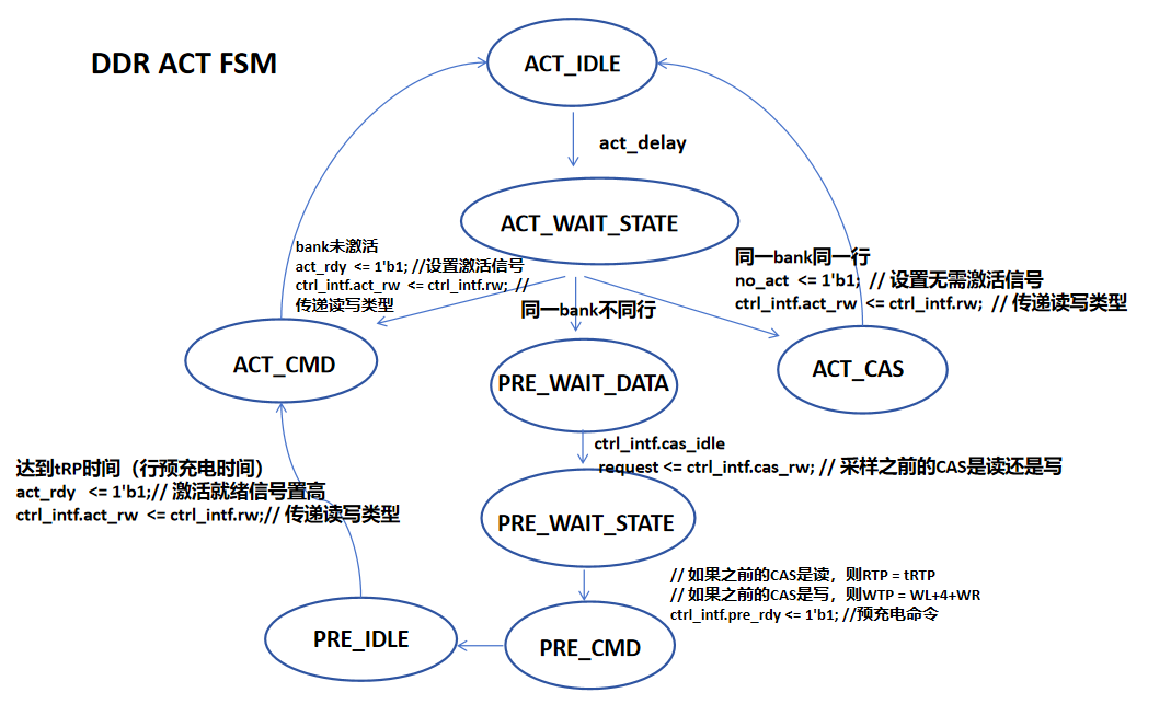
如果有新的 DIMM 访问请求,FSM 就会进入等待状态。这种等待状态是为了满足 tRRD 约束条件。 请求的地址将与存储每个内存组已打开行的表进行核对。
如果访问的 BANK 尚未激活,FSM 将进入 CMD 状态以发送 ACT 命令。
如果访问的是之前已经打开的 ROW,则 FSM 进入跳过 ACT 命令状态(NOTE1)。
如果访问的是同一 BANK 的不同 ROW,FSM 将进入预充电状态(NOTE2)。 在预充状态下,FSM 会等待当前 CAS 完成,并在发出预充命令(NOTE3)前增加写恢复 (tWR) 或读预充 (tRTP) 的延迟。 tRP 之后,FSM 返回 ACT CMD 状态。
同一 BANK 的不同 ROW
步骤1: 预充电 (PRE)
- 命令: 发送预充电命令
- 作用: 关闭当前打开的行(Row A),准备打开新行
- 相关参数:
- 需要等待之前的读/写操作完成
- 如果是读操作后预充电:需要满足 tRTP (Read to Precharge)
- 如果是写操作后预充电:需要满足 tWR (Write Recovery time) + tWTR (Write to Read)
步骤2: 等待 tRP (Row Precharge Time)
- 参数: tRP = 行预充电时间
- 作用: 等待bitlines预充电完成,恢复到稳定的状态
- 典型值: 13-18ns (取决于DDR频率和型号)
- 计算公式: tRP = tRP (时钟周期数 × 时钟周期时间)
步骤3: 激活新行 (ACT)
- 命令: 发送激活命令
- 作用: 打开新的行(Row B),将数据从存储单元传输到sense amplifier
- 条件: 必须在tRP完成后才能发送
步骤4: 等待 tRCD (RAS to CAS Delay)
- 参数: tRCD = 行地址到列地址延迟
- 作用: 等待行激活完成,sense amplifier准备好数据
- 典型值: 13-18ns
- 计算公式: tRCD = tRCD (时钟周期数 × 时钟周期时间)
步骤5: 读/写操作 (RD/WR)
- 命令: 发送读或写命令
- 作用: 访问新行中的数据
- 条件: 必须在tRCD完成后才能发送
DDR CAS 模块 (ddr_cas.sv)
该模块用于实现下面简化的 FSM,以控制 CAS 命令的时序。
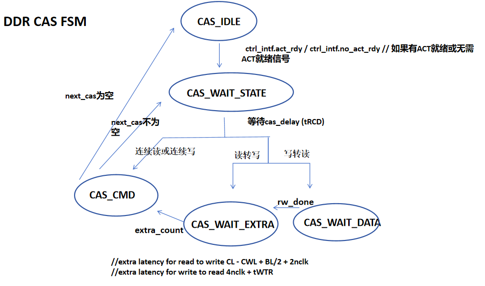
在收到新的 ACT 命令后,FSM 进入等待状态。 等待状态针对 tRCD(ACT 到CAS 的延迟)和 tCCD(CAS 到 CAS 的延迟)。 如果有 “读到写 “或 “写到读 “操作 (tWTR),也需要额外等待。
如果队列中仍有 ACT 命令,状态机将返回等待状态。 该模块中的队列用于在执行前一条 ACT 命令的同时跟踪新的 ACT 命令。 每次从队列中提取 ACT 命令时,都会更新队列中剩余 ACT 命令的等待时间。 等待时间将检查 tRCD 和 tCCD。
DDR RW 模块 (ddr_rw.sv)
该模块简化的状态机如图所示,用于控制发送写入或读取数据的时间。
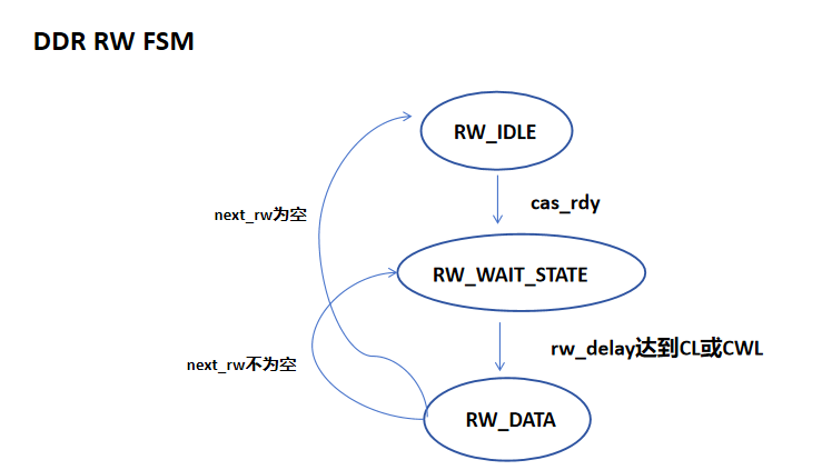
如果有新的 CAS 命令,FSM 将进入等待状态。 等待状态的时间取决于是读操作还是写操作,以满足 CL 或 CWL 的限制。与突发 CAS 模块类似,该模块也使用队列来捕获 CAS 命令,同时执行前一个命令。
DDR 突发数据模块 (burst_data.sv)
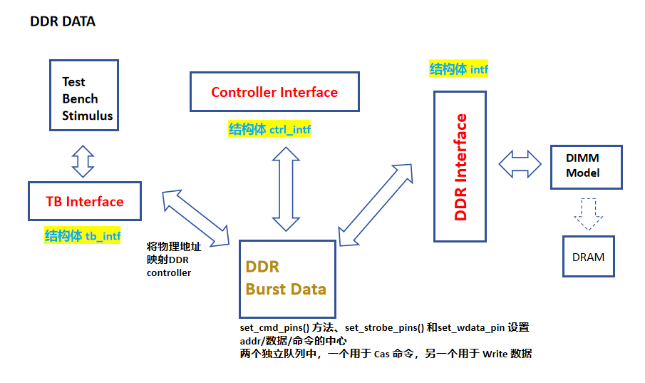
该模块是为 set_cmd_pins() 方法、set_strobe_pins() 和set_wdata_pin 设置 addr/数据/命令的中心。该模块捕捉激励输入,并将其排列在两个独立队列中,一个用于 Cas 命令,另一个用于 Write 数据。 当命令准备就绪时,数据/地址/设置将从队列池中提取并打包到DIMM 命令中。
这个模块是整个DDR控制器的数据枢纽,连接了控制逻辑和物理接口,确保所有命令和数据按照正确的时序发送到DDR设备。
DIMM 模组 (dimm_model.sv)
该模块作为测试台仿真的一部分来实现,以提供存储和检索数据的手段。 模块对信号引脚进行采样,以捕获 ACT 和 CAS 命令中发送的地址以及 DQ 中的数据。 数据以 ACT 和 CAS 中捕获的地址为索引写入关联数组。 在读取操作中,从数组中获取数据,并调用 DDR 接口的方法将其转换为引脚事务。
各个时序顺序整理
ACT_DELAY :ACT命令延迟时间
tRCD : 行激活到列读写命令延迟
tCCD : 列到列读写命令延迟
CWL:写命令到数据输入延迟
CL :读命令到数据输出延迟
第一次读/写
ACT_DELAY —> 等待tRCD —> CL/CWL
① 同一bank不同行
读 / 写 ———> 读 / 写 (连续读 或 连续写)
ACT_DELAY —> 等待 tRTP / tWTP —> 预充电tRP —> 等待tCCD —> CL/CWL
读 / 写 ———> 写 / 读 (读转写 或 写转读)
ACT_DELAY —> 等待 tRTP / tWTP —> 预充电tRP —> 等待tRCD —> extra_count —> CL/CWL
② 同一bank同一行
读 / 写 ———> 读 / 写 (连续读 或 连续写)
ACT_DELAY —> 等待tCCD —> CL/CWL
读 / 写 ———> 写 / 读 (读转写 或 写转读)
ACT_DELAY —> 等待tCCD —> extra_count —> CL/CWL
③ 未激活bank,相当于首次读/写
ACT_DELAY —> 等待tRCD —> CL/CWL
转载请注明来源,欢迎对文章中的引用来源进行考证,欢迎指出任何有错误或不够清晰的表达。可以在下面评论区评论,也可以邮件至 351134995@qq.com